Advanced Semiconductor Packaging – TSV Metrology
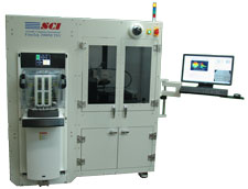
The FilmTek™ 2000M TSV advanced semiconductor packaging metrology system provides an unmatched combination of speed, accuracy, and precision for high-throughput measurements of resist thickness, through silicon vias (TSVs), Cu-pillars, bumps, redistribution layer (RDL) and other packaging processes.
TSV etch depth and depth uniformity is critical to ensure high yield during TSV fabrication. The FilmTek™ 2000M TSV can readily determine etch depth for via structures with diameters greater than 1 µm up to a maximum etch depth of 500 µm. Additional capabilities include measurement of height or depth, critical dimension, and film thickness for microbumps, trenches, and a variety of other structures and applications.
Key Features:
- Measure high aspect ratio TSV structures
- Measure TSV etch depth up to 500 µm
- Measure TSV structures with diameter down to 1 µm
- Patented FilmTek™ technology
- Fast measurement time (~1 second per point)
- TSV etch depth, bump height, critical dimension, and film thickness metrology in a single tool
- Cassette to cassette wafer handling
- Brooks or SCI automation
- 300mm, FOUP, and SMIF compatible
- SECS/GEM
High Aspect Ratio TSV Measurement Methodology
To continue improvements in power efficiency and system performance, semiconductor manufacturers are looking beyond traditional 2D scaling strategies towards 3D integration. Chip stacking using through-silicon-via technology is a key enabling step for 3D-IC integration. The TSV is formed by etching a deep via through silicon, depositing an isolation layer on the via side wall, and filling the via with a conductor material such as copper or tungsten. The TSV can be formed before completion of the device (via first / via middle) or after device formation (via last). To make connections to the TSV, the silicon wafer is thinned down to expose the TSV.
Because the 3D chip stacking is post wafer fabrication, any yield loss due to the 3D integration process will have a significant cost impact on the final system. Since TSV dimensions (microns) differ from typical transistor dimensions (nanometers) by an order of magnitude, additional metrology is required to monitor the TSV fabrication. A quantitative metrology technique that provides non-destructive, high throughput measurements of TSV etch depth and depth uniformity is necessary in the wafer production line to monitor production quality and stability, and to ensure final high device yield.
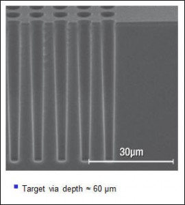
There has been a growing demand for measuring high aspect ratio via structures with diameters less than 30 microns and depths ranging from tens to hundreds of microns. The primary method currently used to measure the etch depth of high aspect ratio TSVs is cross-section scanning electron microscopy (SEM). Because cross-section SEM is time consuming and destructive, it cannot be used as in-line metrology for high volume manufacturing.
Various optical techniques have been developed to detect changes in etch depth for process control, including confocal scanning optical microscopy, optical scatterometry techniques, infrared (IR) reflectometry, top-down IR interferometry, and white light interferometry. Although these techniques are capable of measuring etch depth, they are very sensitive to the aspect ratio and are typically not able to reliably measure TSV structures with CD feature sizes in the 1-10 μm range and etch depth of 20 μm or deeper (aspect ratios greater than 20:1) because of signal attenuation. As the via diameter decreases, the TSV aspect ratio increases and there are few non-contact measurement techniques that are suitable for in line inspection.
SCI has developed a patented optical method based on normal incidence reflectometry to measure the etch depth of high aspect ratio TSV structures. The patented optical design of the FilmTek™ 2000M TSV allows for a very small spot size with a low power objective. For example, the system can be configured such that a 10X objective gives a measurement spot size of 5 µm by 10 µm in the in the y and x dimensions, respectively. Avoiding the use of a high power objective is critical for limiting the angular spectrum of the collected light and maximizing the coherence of the spectral reflection from a high aspect ratio TSV or trench structure.
Optical Etch Depth Measurement of High Aspect Ratio TSV Structures
- Interference between reflected waves is caused by optical path length difference between the top and bottom surfaces of the TSV structure
- The spot size must be small (same order as via diameter) and the measurement beam must be nearly collimated to observe interference in the reflected light
- Patented FilmTek™ technology allows a small measurement spot size without the use of a high power objective
Comparison of Via Etch Depth by FilmTek™ 2000M TSV and SEM
| Via Diameter(µm) | Etch Depth (µm) SEM |
Etch Depth (μm) FilmTek™ 2000M TSV |
|---|---|---|
| 5 | 44.5 | 44.3 |
| 10 | 55.5 | 55.5 |
| 15 | 62.0 | 61.8 |
| 20 | 66.5 | 66.8 |
- Excellent agreement between FilmTek™ 2000M TSV and SEM data

| Technical Specifications | |
|---|---|
| Measurement function: | TSV etch depth, bump height, critical dimension, and film thickness |
| Wafer handling: | Brooks or SCI |
| Substrate size: | 200 or 300mm |
| Pattern recognition: | Cognex |
| CD precision (1σ): | <0.2% |
| Etch depth precision (1σ): | <0.005% |
| Film thickness range: | 5nm to 350µm (5nm to 150µm is standard) |
| Film thickness precision (1σ): | <0.005% |
| Light source: | Halogen lamp |
| Detector type: | 2048 pixel linear CCD array |
| Computer: | Multi-core processor with Windows™ 10 Operating System |
| Wafer throughput: | >60 WPH |


