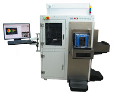
Optical Thin-Film Metrology for Advanced Thin Films
The FilmTek™ 6000 PAR-SE is our most advanced film metrology system for film thickness, refractive index and stress measurement for a broad range of film layers at the 1x nm design node and beyond. The FilmTek™ 6000 PAR-SE accommodates 200 or 300 mm wafer metrology.
The FilmTek™ 6000 PAR-SE combines spectroscopic ellipsometry and DUV multi-angle polarized reflectometry with a wide spectral range to meet the challenging demands associated with multi-patterning and other leading-edge device fabrication techniques.
Manufacturing advanced IC devices at 1x nm design rules requires the use of complex films that must be highly uniform. To maintain tight control over the processes used to build these films requires metrology systems that can monitor extremely thin films that are often within a multi-layer film stack (e.g., high-k and oxide-nitride-oxide Films). Additionally, some processes result in gradients through the thickness of the film that must be monitored for optimum device performance (e.g., implant damage and low-k Films). Existing metrology tools that rely on conventional ellipsometry or reflectometry techniques are limited in their ability to detect film changes for these applications
To meet these challenges, FilmTek™ 6000 PAR-SE combines patented Multi-Angle Differential Polarimetry (MADP) and Differential Power Spectral Density (DPSD) technology to independently measure film thickness and index of refraction. By independently measuring index and thickness, the FilmTek™ 6000 PAR-SE is far more sensitive to changes in films, particularly films within multi-layer stacks, than existing metrology tools that rely on conventional ellipsometry or reflectometry techniques. This is ideal for both ultra-thin and thick multilayer film stacks used in forming complex device structures.
Key Features:
- Spectroscopic ellipsometry with rotating compensator design (295nm-1700nm)
- Multi-angle, polarized spectroscopic reflection (190nm-1700nm)
- Measures film thickness and index of refraction independently
- Multi-Angle Differential Polarimetry (MADP) technology with SCI’s patented Differential Power Spectral Density (DPSD) technology
- Ideal for measuring ultra-thin films (0.03 Å repeatability on native oxide)
- Patented parabolic mirror technology – small spot size measures within a 50×50 µm feature
- Cassette to cassette wafer handling
- Pattern recognition (Cognex)
- FOUP or SMIF compatible
- SECS/GEM
Measurement Capabilities:
FilmTek™ 6000 PAR-SE incorporates SCI’s generalized material model with advanced global optimization algorithms for simultaneous determination of:
- Multiple layer thicknesses
- Indices of refraction [ n(λ) ]
- Extinction (absorption) coefficients [ k(λ) ]
- Energy band gap [ Eg ]
- Composition (e.g., %Ge in SiGex, % Ga in GaxIn1-xAs, %Al in AlxGa1-xAs, etc.)
- Surface roughness
- Constituent, void fraction
- Crystallinity/Amorphization (e.g., degree of crystallinity of Poly-Si or GeSbTe films)
- Film gradient
| Technical Specifications | |
|---|---|
| Film thickness range: | 0Å to 150µm |
| Film thickness accuracy: | ±1.0Å for NIST traceable standard oxide 100Å to 1µm |
| Spectral range: | 190nm to 1700nm (220nm to 1000nm is standard) |
| Measurement spot size: | 50µm |
| Sample size: | 2mm to 300mm (150mm is standard) |
| Spectral resolution: | 0.3-2nm |
| Light source: | Regulated deuterium-halogen lamp (2,000 hrs lifetime) |
| Detector type: | 2048 pixel Sony linear CCD array / 512 pixel cooled Hamamatsu InGaAs CCD array (NIR) |
| Computer: | Multi-core processor with Windows™ 10 Operating System |
| Measurement time: | ~2 sec (e.g., oxide film) |
| Performance Specifications | |||
|---|---|---|---|
| Film(s) | Thickness | Measured Parameters | Precision (1σ) |
| Oxide / Si | 0-1000 Å | t | 0.03 Å |
| 1000-500,000 Å | t | 0.005% | |
| 1000 Å | t , n | 0.2 Å / 0.0001 | |
| 15,000 Å | t , n | 0.5 Å / 0.0001 | |
| 150,000 Å | t , n | 1.5 Å / 0.00001 | |
| Photoresist / Si | 200-10,000 Å | t | 0.02% |
| 500-10,000 Å | t , n | 0.05% / 0.0002 | |
| Nitride / Si | 200-10,000 Å | t | 0.02% |
| 500-10,000 Å | t , n | 0.05% / 0.0005 | |
| Polysilicon / Oxide / Si | 200-10,000 Å | t Poly , t Oxide | 0.2 Å / 0.1 Å |
| 500-10,000 Å | t Poly , t Oxide | 0.2 Å / 0.0005 | |

